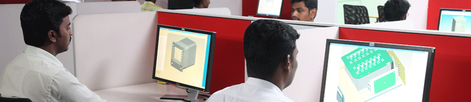
Data Patterns, with years of knowledge and experience in reliable hardware engineering, can offer design and development services for High precision analog, High speed digital, mixed signal and RF design, from elementary boards to high-end complex systems.
Our design philosophy revolves around:
- Re-usability – Quick product development
- Scalability – Seamless enhancement
- Adaptability – Various Platforms
- Interoperability – Co-existence
- Testability – Test coverage and diagnostics
- Maintainability – Long term support and protection against obsolescence
Data Patterns’ ability to not only design the product but to also manufacture the first prototypes, test the product, provide first article inspection services, and undertake production runs, all within the same establishment, offers a significant advantage of single point communication, and consequently, flawless synergy with you.
Our domain exposure includes Embedded Systems, Communication Systems, Signal processing Systems, Control Systems, Navigation and Radar processing. We are experts in these domains, and boast of the ability to develop supporting algorithm development, simulation and validation for the desired end use. To support our design and delivery, we are exceptionally competent in Mathematical Modeling, Data analysis, Feasibility checks, System development, System and Performance analysis, and rapid prototyping.
When required, for realizing hardware design, high reliability processes to eliminate error progression are followed in Data Patterns. Events such as Power Analysis, Thermal Analysis, Structural Analysis, FMECA (Failure Mode Effect and Criticality Analysis) and MTBF (Mean Time Between Failures), act as gates to design reliability into the product.
We carry out Physical, Data Link and Control Interface Layers design. Our expertise in designing standard boards such as VPX, VME, FMC, XMC , PMC, cPCI, COMe, etc., is proven and established. We are able to design boards that involve High speed Processors, FPGAs, DAC/ ADC, DDR II , DDR III, QDR , Ethernet, PCIe, and USB devices.
Our portfolio of Board Design Competencies can be categorized as:
- High Density / Complex Digital.
- High Precision Analog / Mixed Signal.
- Power Supplies.
- RF/IF Design
- Backplane Modules.
- Rigid-Flex.


Data Patterns design and development processes have been validated by international customers. Good product realization practices such as release of BOMs at 3 stages, preliminary, interim and final, aid smooth timely sourcing of components, and therefore, quick turnarounds. Early kick-off for procuring long-lead time components is ensured by advance selection and sourcing of critical components by our supply chain experts aimed at avoiding delays downstream.
Our designers have also developed an in-house tool for calculating cumulative derating, loading and signal integrity, to ensure the right components are used for the desired optimum performance. Signal integrity checks are carried out both Pre and Post PCB routing. Additionally, simulation to capture overshoot, delays, cross talk, ringing, signal rise/ fall time, using Mentor Graphics applications, allows us to pre-empt problems and increase reliability of the board.
Checklists, Guidelines and templates e.g. routing guidelines for trace width and adjacent tracks separations, enable timely course corrections and further mitigate the risk of downstream errors and delays. An active Design Review Board, composed of cross-functional experts, oversee the project and institute timely problem solving measures,
The statistics on our PCB Design Capabilities speaks for our pioneering zeal and perseverance, as an Indian company, deeply invested in ensuring we deliver the best of the best products globally:
PCB STATISTICS
- Maximum No Layers 22
- Board Thickness 0.35 – 5.4 mm
- Copper Thickness 0.5 – 3oz
- Maximum Board Area 290 X 303 (mm)
- Maximum no of Pins 23500
- Minimum trace width 3
- Minimum trace clearance 3
We also confidently claim our place as experts in Via Technology as well. A sample menu of characteristics achieved is:
- Micro Via / Blind Via Min 4 mil (Laser drill)
- Buried Via Min 8 mil
- Through Hole Via Min 8 mil
- Surface finish ENIG, HASL
- Output Gerber RS-274-X , ODB++
If there is a design or board standard out there, we, in all probability, already have the expertise and capability to ramp-up quickly. For a listing of standards in board design and development that we have exposure in, click here. In the final analysis, a product can only be as good as the people who produce it. To this end, we deploy personnel experienced in a plethora of software tools. A sampling of tools that we use in the design and simulation are as below:
DESIGN- Central Library Management: Mentor Graphics-Library Manager
- Schematic Design: Mentor Graphics -DxDesigner
- Layout Design: Mentor Graphics-Expedition PCB
- Layout Verification: Mentor Graphics -Hyperlynx DRC
- Output: PCB and OrCAD Gerbtool
- Structural Analysis: ANSYS
- Pre-Layout Simulation: Hyperlynx Signal Integrity LineSim
- Post-Layout Simulation: Hyperlynx Signal Integrity BoardSim
- Power Analysis: Hyperlynx Power Integrity
- RF simulation: Advanced Design Systems (ADS)-Agilent Technologies
- Thermal Simulation
Effective use of DRB (Design Review Board) CMO (Configuration Management Office), FAB (Failure Analysis Board) and SAB (Salvage Analysis Board) ensures learning is looped back into the system, continuously enhancing our expertise and ability to support the desired performance objective, including extended use. DRB reviews the PCB for in-depth functional, performance, reliability, safety, testability, standardization, and manufacturability. It provides cross-functional assessment and recommendations. CMO is a single point version control and traceability entity that ensures extensive documentation, which is archived for ease of retrieval, and allows for the maintenance of the system, even with change of support personnel. FAB and SAB captures, and grows, our knowledge base to preempt and prevent failures.
If you need a vendor who understands your PCB requirements, simple and complex, and supplies the product with professional empathy, it’s more than likely that we are the people who can deliver.